
The material modification under picosecond UV emission is important for 3D-binary data storage and direct writing of gratings in optical waveguides. Internal processing of glass and other dielectrics includes a change of refractive index, local melting, etc. The mechanism of internal processing is two-photon absorption and avalanche ionization in the field of picosecond UV pulses. The shorter the laser pulse, the more energy density is absorbed and the faster material modification can be achieved.
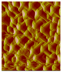
An example is the structuring a Si-wafer surface (B. N. Walker, G. Pasmanik, A. Vertes, American Physics Society Ann. Meeting, Abstract C1.00167, New Orleans, LA, March 10, 2000). The Si-wafer, being illuminated by UV picosecond pulses, changes the surface morphology and, depending on processing conditions, acquires micro-column structures (see left). This is particularly true for fabrication of Si matrices, replacing liquid matrices. It allows users to identify the results of mass spectra measurements more easily because of a lack of complex matrix fragments overshadowing the analyte identification.
As another example, Passat Compiler DPSS picosecond laser was successfully used for Laser Annealing by National Technical University of Athens. See the extract and link below:
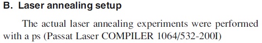
(The citation above is from the article: “Picosecond and nanosecond laser annealing and simulation of amorphous silicon thin films for solar cell applications”, I. Theodorakos1, I. Zergioti1, V. Vamvakas2, D. Tsoukalas1 and Y. S. Raptis)