01 · Two-Photon Absorption in Wide-Bandgap Dielectrics
At sufficiently high peak intensity, a material can absorb two 213 nm photons simultaneously. Each photon carries approximately 5.82 eV, giving a combined excitation energy of 11.64 eV. This is sufficient to bridge the bandgap of most commonly used optical and technical dielectrics, including materials with bandgaps close to 10 eV.
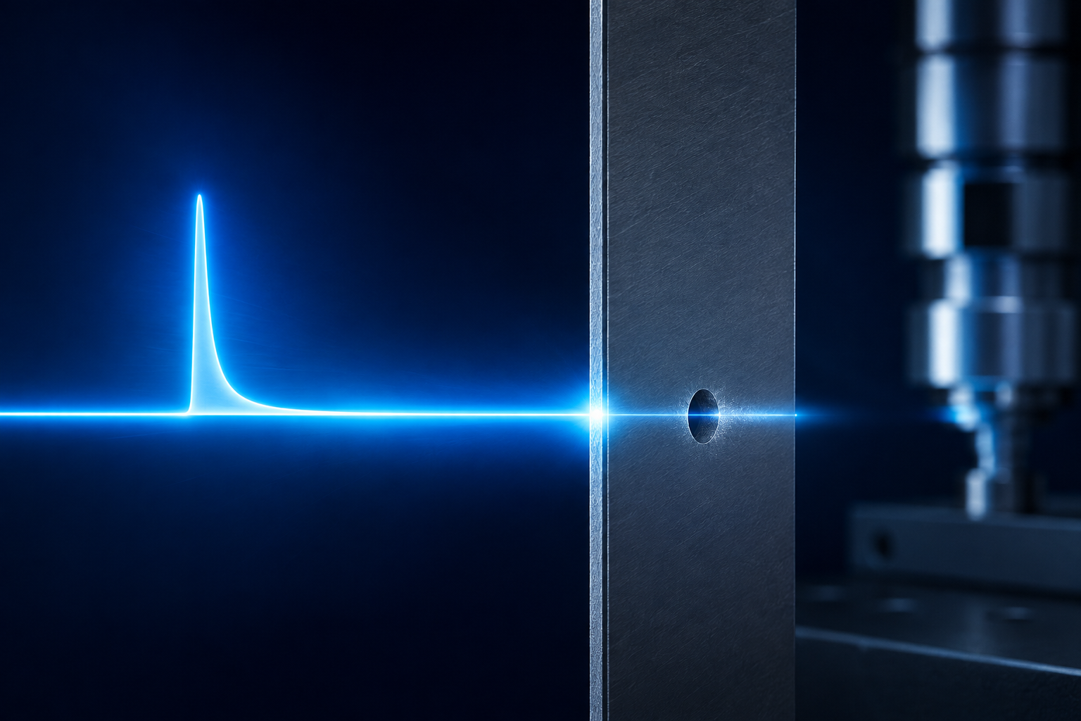
UV-grade fused silica is an especially demanding material to process. Its high purity and very low concentration of absorbing impurities give it excellent ultraviolet transmission, so ordinary linear laser absorption is extremely weak. Under the high peak intensity of a 213 nm picosecond pulse, however, two photons provide 11.64 eV and nonlinear two-photon absorption makes the irradiated focal volume effectively opaque. Energy is then deposited only where the beam is focused, enabling localized ablation, drilling and micromachining through an otherwise transparent substrate.
This high purity is precisely why UV-grade fused silica is valuable for photonics and advanced electronics: it provides low optical loss and contamination, very low thermal expansion, high dimensional and thermal stability, and favorable dielectric performance. The same general challenge applies to other high-purity wide-bandgap dielectrics: fewer defects and impurities improve their functional properties, but also remove the absorption sites that conventional lasers rely on. The 213 nm two-photon process provides a direct way to machine these cleaner and more valuable materials.
| Example dielectric |
Approx. bandgap |
213 nm two-photon energy |
Typical applications |
| UV-grade fused silica (SiO₂) |
8.9–9.0 eV |
11.64 eV |
DUV optics, photomasks, glass interposers and microfluidic chips |
| Sapphire (Al₂O₃) |
8.8–9.0 eV |
11.64 eV |
LED substrates, optical windows, sensors and RF electronics |
| Beryllium oxide (BeO) |
≈10.6 eV |
11.64 eV |
Heat-spreading substrates for high-power RF and microwave electronics |
| Aluminum nitride (AlN) |
6.0–6.2 eV |
11.64 eV |
Power-electronics substrates, LED modules and thermal-management components |
| Magnesium oxide (MgO) |
≈7.8 eV |
11.64 eV |
Insulating substrates, protective coatings and magnetic-memory tunnel barriers |
Representative values; the exact bandgap depends on material composition, structure and measurement method.
1064 nm is one of the most widely used wavelengths for laser drilling, but each photon carries only about 1.17 eV. That photon energy is far below the approximately 9 eV bandgap of high-purity fused silica and is poorly suited to direct processing of transparent wide-bandgap dielectrics. By comparison, two 213 nm photons provide 11.64 eV, allowing strong localized nonlinear absorption at the focus.