APPLICATION EXAMPLES
What our lasers can do
Passat picosecond DPSS laser systems are designed for precision micromachining where conventional methods reach their limits. Ultrashort pulses, high peak power, excellent beam quality and wavelengths from infrared to deep ultraviolet enable accurate processing of metals, semiconductors, ceramics, glass, fused silica, polymers and other advanced materials.
PRECISION MICROMACHINING
One platform. Many materials and processes.
The same Passat laser platform can be configured for micro-drilling, precision cutting, surface texturing, laser marking, engraving, patterning and fabrication of complex microstructures.
Depending on the material and process, features can range from several millimeters down to only a few micrometers while maintaining high dimensional accuracy, clean edges and a minimal heat-affected zone. The examples below show only part of what can be achieved with Passat laser systems.
EXAMPLE 01
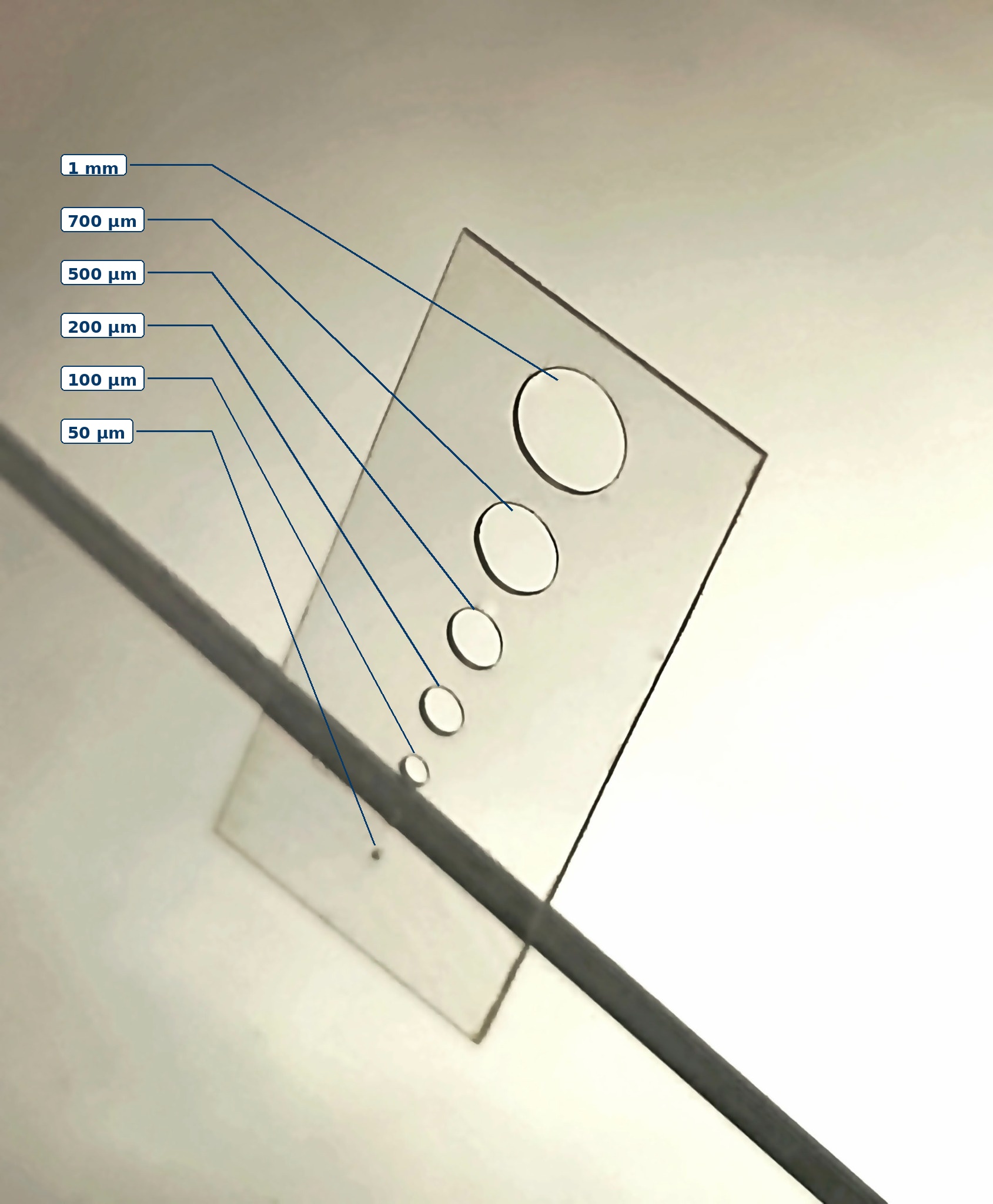
Micro-drilling of thin fused silica
Deep-UV picosecond laser light provides a strong advantage when machining transparent dielectric materials such as fused silica and quartz. The short pulses limit thermal loading and mechanical stress, making it possible to drill extremely thin and fragile substrates that are difficult or impossible to process with conventional drills or cutting tools.
EXAMPLE 02
Surface micro-engraving on glass
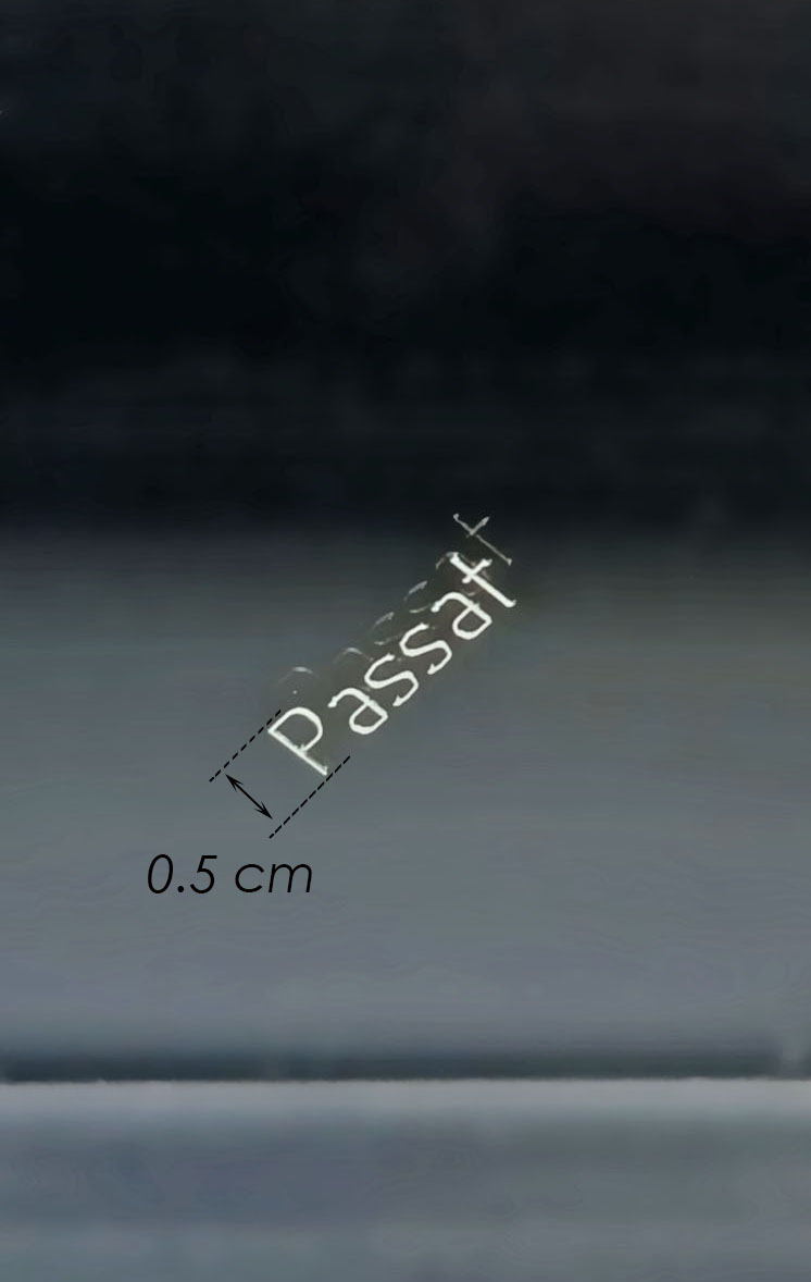
Picosecond UV pulses can create fine, permanent markings directly on a glass surface. The small focused spot and controlled material removal enable clear lettering and patterns while limiting cracking and heat damage in the surrounding area.
This approach is suitable for identification marks, optical components, laboratory devices, precision scales, logos and other small features where conventional engraving would be too coarse or mechanically stressful.
EXAMPLE 03
Microscale relief engraving on glass
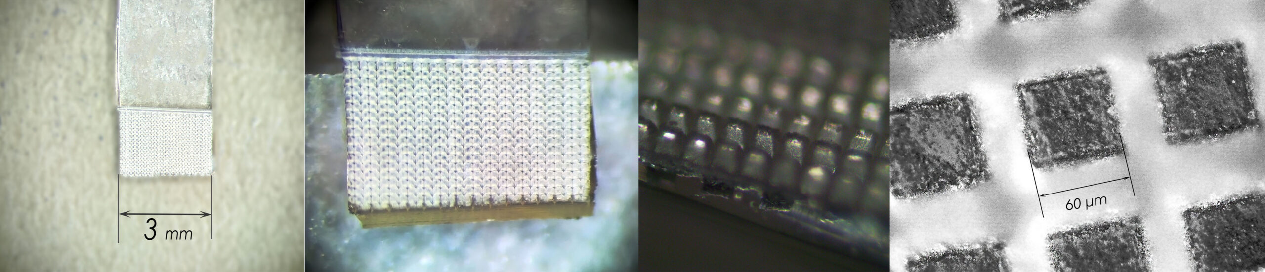
Passat picosecond UV lasers can create regular three-dimensional microrelief patterns directly on glass surfaces. The short pulse duration and small focused spot allow dense arrays of accurately positioned features to be produced while limiting cracking and thermal damage in the surrounding material.
In this example, a square grid was engraved into glass over a total width of approximately 3 mm. Each individual square measures approximately 60 × 60 µm, with an engraving depth of about 60 µm.
EXAMPLE 04
Microscale relief engraving on aluminum
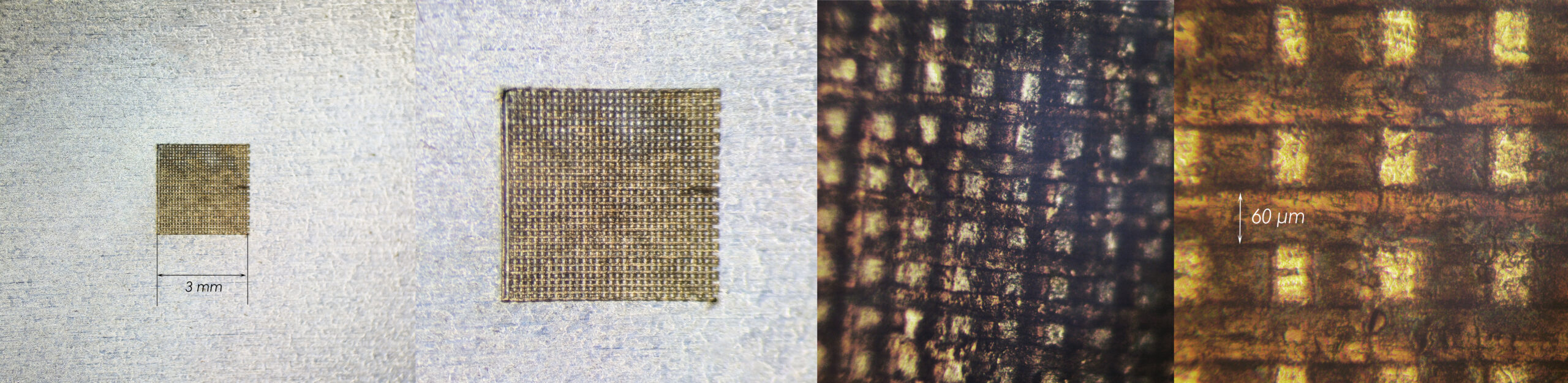
The same microrelief patterning approach can also be applied to metals. In this example, a regular square grid was engraved into an aluminum surface using picosecond laser pulses.
The patterned area is approximately 3 mm wide. Individual square features are approximately 60 × 60 µm, demonstrating repeatable microscale surface structuring across a dense array.
EXAMPLE 05
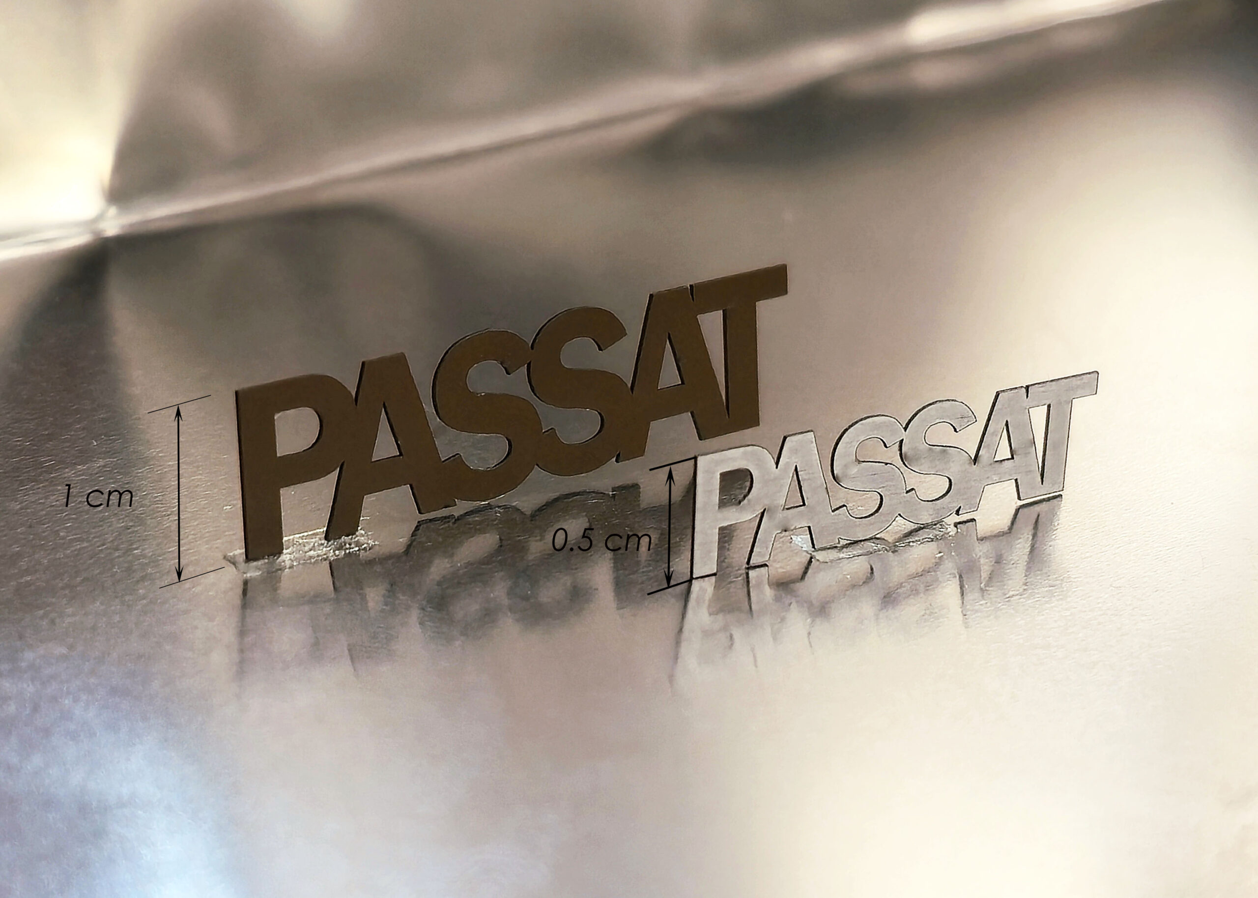
Precision cutting of thin aluminum sheets
Passat picosecond laser systems can cut complex shapes from thin metal sheets with high dimensional accuracy and a narrow kerf. The short pulse duration limits heat transfer into the surrounding material, helping preserve sharp edges and small geometric details.
In this example, the word “PASSAT” was cut from a 250 µm thick aluminum sheet in two sizes. The letter heights are approximately 10 mm and 5 mm.
EXAMPLE 06
High-speed drilling in metal foils
The Compiler HPRR extends Passat picosecond micromachining capabilities to higher-throughput processing. Its high repetition rate enables rapid drilling of thin metal foils while maintaining the dimensional accuracy and limited heat-affected zone associated with picosecond pulses.
Operating at repetition rates up to 12,000 Hz, the platform is suitable for high-speed drilling, wafer processing, semiconductor scribing, precision cutting and other industrial micromachining applications.
Demonstration of high-speed drilling in thin metal foils using the Compiler HPRR at 266 nm, 10 µJ pulse energy, 5 ps pulse duration and 14 kHz repetition rate.
MORE EXAMPLES TO COME
A growing library of real machining results
This page will be expanded with additional examples of metal cutting, metal micro-drilling, ceramic processing, tungsten carbide machining, semiconductor processing, surface texturing and other applications.