Precision processing beyond conventional limits

OUR
TECHNOLOGIES
& ADVANTAGES

Picosecond deep-UV laser systems for the materials, feature sizes and emerging processes that challenge conventional machining.

ns ps fs Energy · precision · deep UV
Why Picosecond Pulses?

High peak power with practical pulse energy

The Picosecond
Advantage

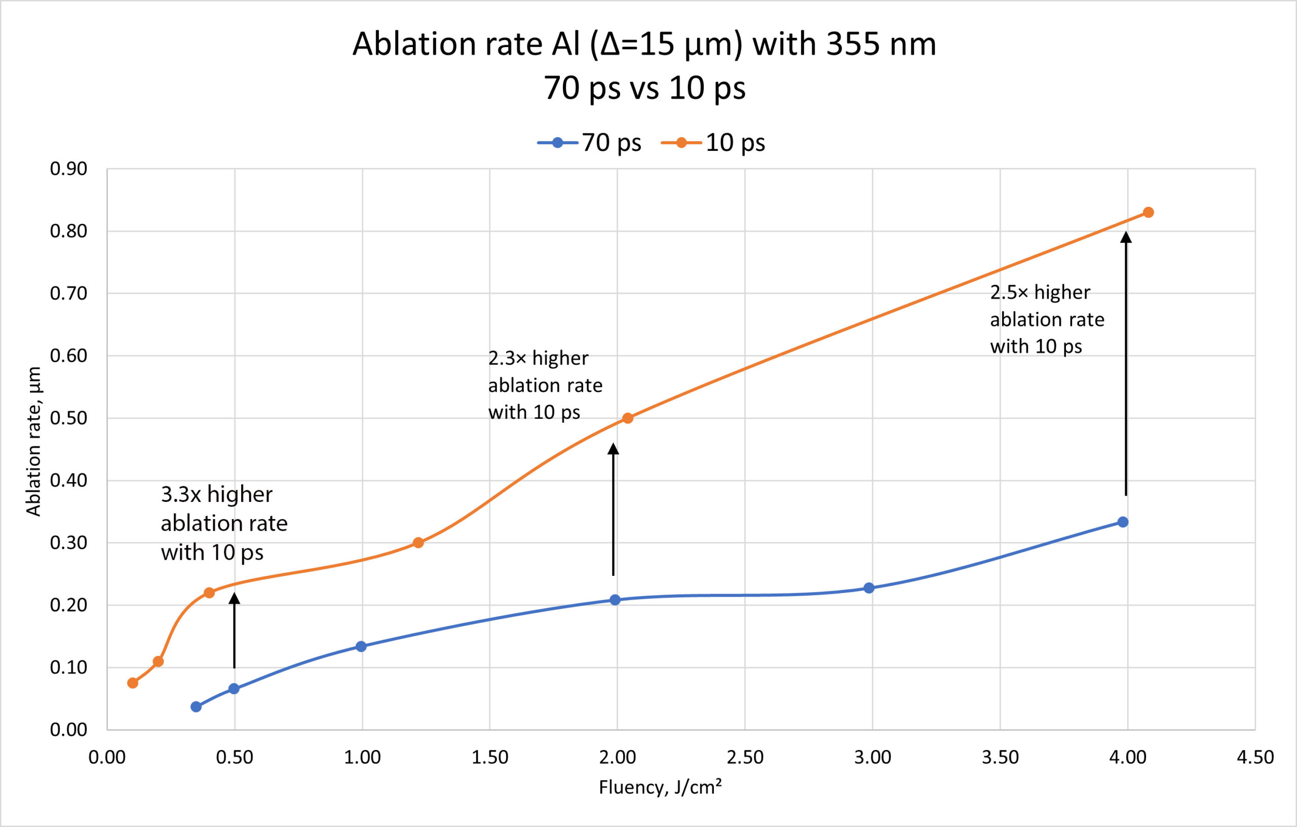
Peak power is determined by how much pulse energy is delivered within the pulse width. A picosecond laser can therefore reach very high peak power without requiring the much larger pulse energy needed by a nanosecond source.

Picosecond operation provides a practical combination of high peak power, useful pulse energy and efficient conversion from IR to UV and deep UV. It supports effective material removal while keeping the laser system considerably more compact than a nanosecond source designed to reach comparable peak power.

ns

Nanosecond

Much more energy required for the same peak power

Because a nanosecond pulse is hundreds or thousands of times longer, reaching the same peak power requires correspondingly greater pulse energy. Generating and handling that energy increases the required gain volume, pump power, cooling, optical aperture and overall system size and cost. Greater optical loading also accelerates degradation of nonlinear crystals, coatings and other optical components. The longer pulse additionally allows more heat to spread into the material.

ps

Picosecond

High peak power without excessive pulse energy

Picosecond pulses reach high peak power with substantially lower pulse energy than nanosecond sources. This enables efficient ablation in a more compact system, reduces the energy load on the optics and limits heat diffusion, helping produce cleaner edges with less melting and recast.

fs

Femtosecond

Excellent confinement, inefficient deep-UV conversion

Femtosecond lasers operate primarily in the IR and green spectral ranges. Further conversion into the UV is highly inefficient and technically difficult, while operation at these converted wavelengths can be considerably less stable. The additional conversion stages also reduce the usable pulse energy and increase the complexity and cost of the system. As a result, commercial femtosecond lasers are rarely used in the UV and are particularly uncommon in the deep-UV range.

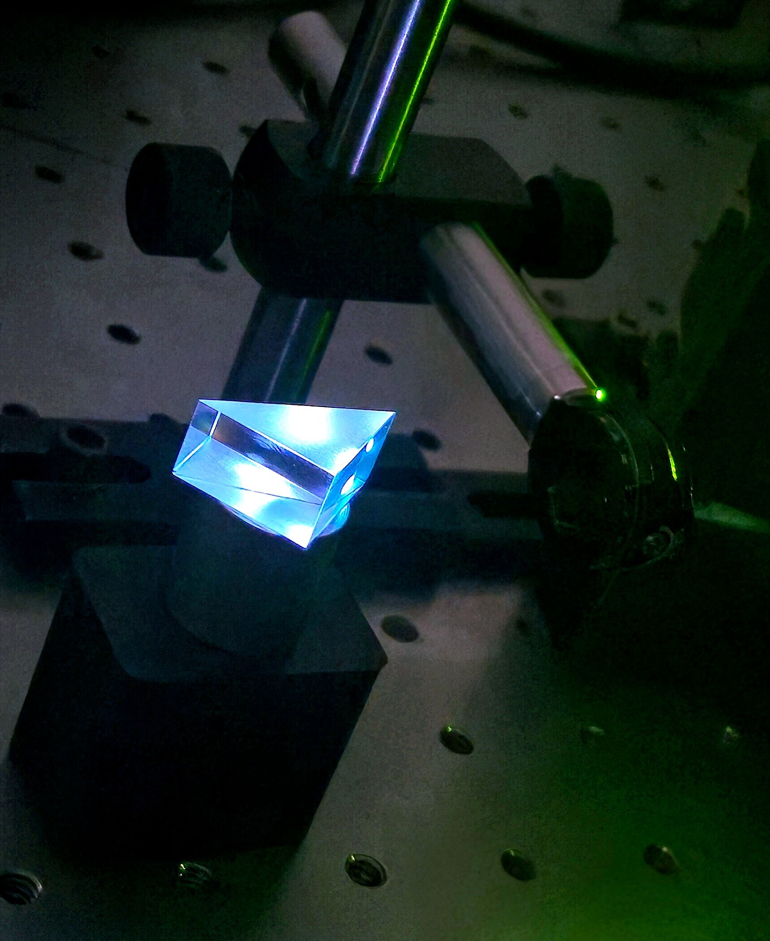
Deep-UV laser light visible in a prism
213 nm 5.82 eV per photon

Why deep UV?

More Energy Per Photon.
A Smaller Focal Spot.

At 213 nm, each photon carries approximately 5.82 eV. Two-photon absorption can bridge the approximately 9 eV bandgap of fused silica, whereas excitation at 1064 nm requires a much higher-order multiphoton process.

Deep UV can therefore couple energy more efficiently into transparent dielectrics, many ceramics and semiconductor structures. The shorter wavelength also supports tighter focusing, enabling micron-scale features with lower pulse energy and less damage to surrounding material.

Two-photon absorption in fused silica Improved coupling in wide-bandgap materials Micron-scale focusing and features Compact all-solid-state alternative to excimer DUV
Where Industry Is Moving

Smaller · thinner · more integrated

The Next Generation
of Precision Manufacturing

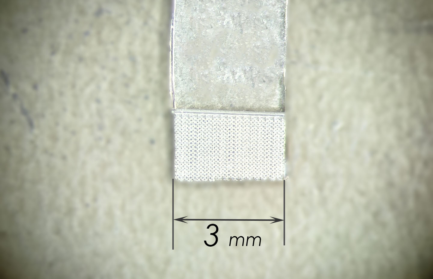
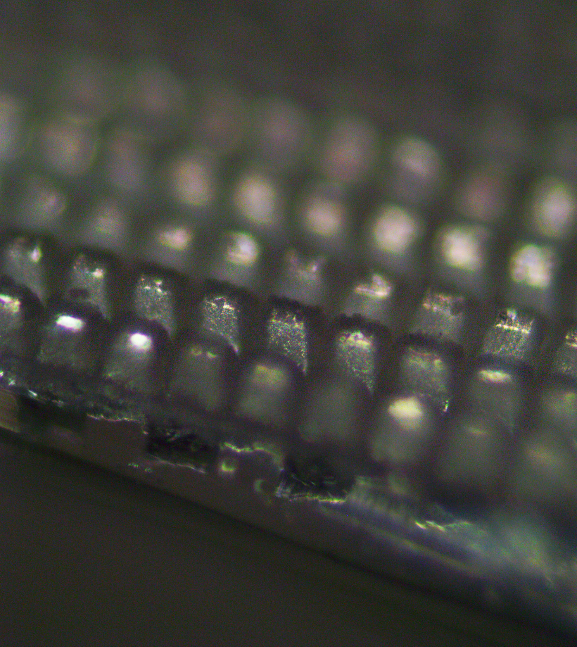
Three millimeter microstructured area on glass Microscope view of the microstructure

All modern technologies are moving toward smaller dimensions. In microelectronics, reducing the size of components also reduces the distance between functional nodes, allowing signals to reach their destinations faster and improving the speed and accuracy of information processing.

This trend extends far beyond electronics. In medicine, for example, minimally invasive instruments, microneedles, implantable sensors and microfluidic diagnostic devices depend on smaller and more precise components to improve performance while reducing trauma to the patient.

These developments require highly accurate microstructures, clean edges, small holes and controlled material removal. Lasers are especially well suited to these tasks because they provide non-contact processing, can be focused into a very small spot, offer precise control of the delivered energy and can machine a wide range of materials while minimizing mechanical stress and thermal damage.

Smaller features

Mechanical tools and long-wavelength beams reach practical limits in diameter, kerf width and placement density.

More difficult materials

Transparent dielectrics, ceramics and superhard materials absorb poorly or crack under conventional processing.

Less tolerance for heat

Thin wafers, coatings and multilayer structures can be damaged by melting, recast and thermal stress.

Cleaner production

Manufacturers seek fewer chemical stages, less tool wear and compact, maintainable equipment.

Future-facing applications

Technologies Where
Passat Lasers Can Lead

The following processes can benefit from picosecond pulse width, high pulse energy, configurable pulse control and wavelengths extending to 213 nm.

Advanced packaging · MEMS · microfluidics

Precision Drilling of Thin Fused Silica and Glass

Thin fused silica and glass plates around 100–300 µm are increasingly used in advanced packaging, sensors, photonics and lab-on-a-chip devices. These applications require dense arrays of small through-holes with clean edges and reproducible geometry.

Current approaches and limitations

Ultrasonic drilling is limited by tool wear and minimum diameter. Excimer systems require gas handling. Femtosecond LIDE and FLICE normally add chemical etching, while plasma and wet etching require masks, vacuum equipment or aggressive chemistry.

Where Passat can provide an advantage

A 213 nm picosecond laser offers direct, mask-free drilling. Two-photon absorption supports interaction with fused silica; tighter focusing enables small holes; and picosecond pulses help limit cracks, chipping and heat-affected material without a mandatory chemical post-process.

Semiconductor repair · selective processing

Local Coating Removal from Semiconductor Wafers

Semiconductor production requires removal of particles, photoresist residues, defective coating areas and thin functional layers without damaging the wafer or existing micro- and nanostructures.

Current approaches and limitations

Wet chemistry processes the whole wafer and creates waste. Plasma can alter surface chemistry. Direct laser cleaning is localized, but the window between removing a thin layer and damaging the substrate can be narrow. Conventional laser-shock cleaning mainly removes weakly attached particles.

Where Passat can provide an advantage

A future approach is localized removal using a picosecond-generated shock wave. The laser ablates an auxiliary foil or intermediate layer rather than the functional wafer surface; the resulting mechanical pulse can separate a selected coating area while reducing direct heating of the substrate.

Research / future development direction

Thin films · photonics · functional materials

Pulsed Laser Deposition

PLD transfers material from a laser-ablated target to a substrate and is used for complex oxides, optical coatings, semiconductor layers, sensors and research-scale functional films.

Current approaches and limitations

KrF and ArF excimer lasers are established PLD sources but use gas mixtures and high-voltage equipment. UV Nd:YAG systems are simpler, although longer wavelengths can require higher fluence. Femtosecond PLD can reduce droplets but uses more complex, costly sources.

Where Passat can provide an advantage

Picosecond 213 nm operation can occupy the middle ground: efficient DUV absorption and stable plasma formation in a compact all-solid-state platform, without an excimer gas system. Picosecond timing reduces target heating while retaining useful pulse energy.

Future analytical systems · plasma research

Laser-Induced X-Ray Spectroscopy

A high-peak-power pulse focused on a target can form a dense plasma that emits characteristic X-rays. Detecting this emission may provide localized elemental information from metals, minerals, ceramics and composites.

Current approaches and limitations

XRF needs an X-ray tube or isotope source. LIBS is fast and remote but analyzes crowded optical spectra. SEM/EDS offers high spatial resolution but requires expensive vacuum equipment and is unsuitable for rapid analysis of large objects.

Where Passat can provide an advantage

High pulse energy and picosecond peak power are attractive for creating highly ionized plasma in a small volume. The 213 nm wavelength can improve energy coupling. This remains a research direction that may eventually combine localized laser processing and elemental analysis.

Research / future development direction

Tooling · electronics · aerospace

Micromachining of Superhard and Brittle Materials

Tungsten carbide, technical ceramics, sapphire, silicon nitride and polycrystalline diamond offer exceptional hardness and wear resistance—but those same properties make small holes and complex features difficult to manufacture.

Current approaches and limitations

EDM works only with conductive materials, can be slow and leaves a modified surface layer. Diamond grinding creates mechanical load, tool wear and chipping. Many ceramics absorb 1064 nm poorly, so infrared processing can require higher fluence or more pulses.

Where Passat can provide an advantage

Deep-UV laser light is absorbed more efficiently by many ceramics and wide-bandgap materials. A smaller focal spot improves resolution, while picosecond pulses limit heat diffusion and reduce cracks, chipping and thermally modified material.

Microelectronics · power devices · photovoltaics

Semiconductor Wafer and Solar-Cell Processing

Wafer dicing and solar-cell separation require narrow kerfs, high positional accuracy and minimal edge damage. The challenge increases for thin silicon and hard, brittle wide-bandgap materials such as SiC and GaN.

Current approaches and limitations

Diamond blades create particles, tool wear and mechanical cracks. Stealth dicing depends on internal transparency and precise focusing. Infrared laser cutting is contactless but can produce a larger heat-affected zone and couples inefficiently into some wide-bandgap materials.

Where Passat can provide an advantage

The 213 nm wavelength provides a smaller focal spot and stronger absorption in many semiconductor and coating materials. Picosecond pulses reduce heat diffusion, helping limit melting, chipping and microcracks in thin wafers and next-generation power devices.

Micro-nozzles · filters · masks · miniature devices

Metallic Microstructures

Modern precision systems require holes, slots, grids and free-form metal features from several tens to several hundreds of micrometres, often in thin foils and miniature parts.

Current approaches and limitations

Mechanical micromachining is limited by tool wear, burrs and feature size. Micro-EDM works only with conductive parts and can be slow. IR lasers may melt edges; nanosecond UV improves resolution but still leaves appreciable thermal effects.

Where Passat can provide an advantage

Picosecond 213 nm operation combines the small focal spot of deep UV with reduced heat diffusion. It can produce narrow cuts and repeatable microholes with less recast, burr formation and edge melting, without mechanical contact or electrode wear.

START A CONVERSATION

What does your application
require?

Tell us about the material, thickness, feature size and required process result. We will help identify a suitable laser configuration.

GO TO CONTACT PAGE